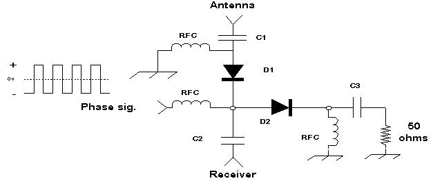
This circuit uses two diodes which act as switches to the rf energy from the antenna or resistor. When a diode is forward biased the rf passes through relatively unimpeded. The reverse biased diode, however blocks most of the rf energy. The RF chokes in this circuit provide DC paths need for the diodes.
Below is Bob's circuit (though I don't know that he actually invented it). It also uses diodes as switches but uses quarter wave transmission lines instead of lumped inductance chokes. Bob's circuit has the advantage at UHF and microwave where strip-line techniques could be utilized to preserve impedances without the lumped values introduced by the chokes.

Just Remember that a quarter wavelength line which is shorted at the
far end looks like an open, that is invisible from the near end, and a
quarter wavelength line which is open at the far end looks like an rf short
to ground at the near end at the frequency of operation. Each of the four
representations is a simplification of the one above it.

L1 - L4 are quarter wavelength sections..
In the top diagram (A) the input voltage from the square wave generator is positive. This forward biases the diode on the left but not the one on the right because it faces into the positive voltage. The diode on the left thus connects the input capacitor to L3, giving an rf short to ground which is symbolized by the dotted line (A1). From the antennas end of L3, the shorted quarter wavelength section seems to disappear (A2). Since the diode on the right goes nowhere (as far as RF is concerned), L4 looks like an open quarter wavelength section to the resistor, and thus an rf short to ground (A3). Because L2 now looks shorted to ground at the far end from the receiver's perspective, it becomes invisible to the receiver (A4). Thus we are left in this state with the antenna connected to the receiver via L1.
Now in diagram B, we have a negative with respect to ground voltage applied to the diodes. The diode on the right now conducts and appears as an RF short and the one on the left becomes reversed biased and appears as an open (B1). L4 now disappears from the resistors perspective (B2). The antenna now faces into L3 which looks like an RF short so the antenna node becomes RF shorted to ground (B3). Finally, the receiver can no longer see the L1 because it is shorted at the antenna node. We are left in this switching state with the receiver seeing only the terminating resistor.
This strikes me as an elegant solution.
Note that no blocking caps are shown in Bob's circuit at the antenna
or receiver and these would have to be introduced if there were DC paths
to ground in either.